Writers: R.C. Deus and R.A.C. Amoresi and P.M. Desimone and F. Schipani and L.S.R. Rocha and M.A. Ponce and A.Z. Simoes and E. Longo
Keywords: A. Films; B. Defects; C. Chemical properties; D. CeO2; E. Sensors
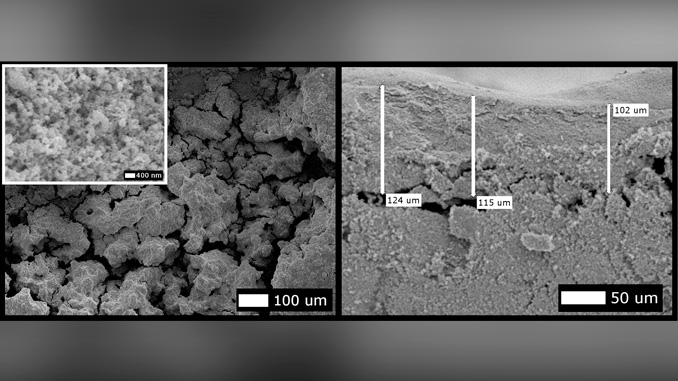
Abstract: Here we present an easy-reproducible microwave-assisted hydrothermal route for preparing pure nanocrystalline CeO2 films. The produced materials were characterized using a wide range of techniques (X-ray diffraction, field emission gun scanning electron microscopy, Raman spectroscopy) to understand the synthesis dependent changes in crystallographic structure, and crystallite size. Raman and X-ray diffraction techniques revealed that the films were free of secondary phases and that they crystallize in the cubic structure. The observed hydrodynamic particle size larger than the crystallite size confirms the aggregation phenomenon. Gas sensing measurements have been carried out to rationalize the type and number of surface adsorbed groups and overall nanostructure. Electrical conductance variations, owing to gases adsorption onto semiconductor oxide films surfaces, were observed in this work. Chemiresistive CeO2film properties depend on the intergranular barrier heights and width.


