Writers: R. A. Simon, H. Kamimura, O. M. Berengue, E. R. Leite, A. J. Chiquito
Keywords: nanowires; devices
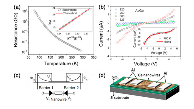
Abstract: It has been demonstrated that the presence of oxide monolayers in semiconductor surfaces alters the electronic potential at surfaces and, consequently, can drastically affect the electronic transport features of a practical device such as a field effect transistor. In this work experimental and theoretical approaches to characterize Al/germanium nanowire Schottky devices by using samples covered with a thin oxide layer (2 nm width) were explored. It was also demonstrated that the oxide layer on Ge causes a weak dependence of the metal work function on Schottky barrier heights indicating the presence of Fermi level pinning. From theoretical calculations the pinning factor S was estimated to range between 0.52 and 0.89, indicating a weak Fermi level pinning which is induced by the presence of charge localization at all nanowires’ surface coming from interface states.
See PDF: Disorder induced interface states and their influence on the Al-Ge nanowires Schottky devices
DOI: 10.1063/1.4857035


